
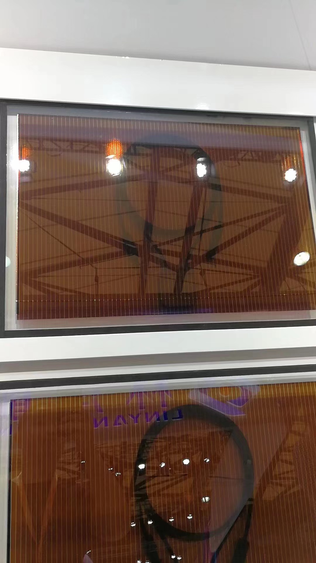
In the photovoltaic industry, perovskite has been in hot demand in recent years. The reason why it has emerged as the “favorite” in the field of solar cells is due to its unique conditions. Calcium titanium ore has many excellent photovoltaic properties, simple preparation process, and a wide range of raw materials and abundant content. In addition, perovskite can also be used in ground power plants, aviation, construction, wearable power generation devices and many other fields.
On March 21, Ningde Times applied for the patent of “calcium titanite solar cell and its preparation method and power device”. In recent years, with the support of domestic policies and measures, the calcium-titanium ore industry, represented by calcium-titanium ore solar cells, has made great strides. So what is perovskite? How is the industrialization of perovskite? What challenges are still facing? Science and Technology Daily reporter interviewed the relevant experts.
Perovskite is neither calcium nor titanium.
The so-called perovskites are neither calcium nor titanium, but a generic term for a class of “ceramic oxides” with the same crystal structure, with the molecular formula ABX3. A stands for “large radius cation”, B for “metal cation” and X for “halogen anion”. A stands for “large radius cation”, B stands for “metal cation” and X stands for “halogen anion”. These three ions can exhibit many amazing physical properties through the arrangement of different elements or by adjusting the distance between them, including but not limited to insulation, ferroelectricity, antiferromagnetism, giant magnetic effect, etc.
“According to the elemental composition of the material, perovskites can be roughly divided into three categories: complex metal oxide perovskites, organic hybrid perovskites, and inorganic halogenated perovskites.” Luo Jingshan, a professor at Nankai University’s School of Electronic Information and Optical Engineering, introduced that the calcium titanites now used in photovoltaics are usually the latter two.
perovskite can be used in many fields such as terrestrial power plants, aerospace, construction, and wearable power generation devices. Among them, photovoltaic field is the main application area of perovskite. Calcium titanite structures are highly designable and have very good photovoltaic performance, which is a popular research direction in photovoltaic field in recent years.
The industrialization of perovskite is accelerating, and domestic enterprises are competing for the layout. It is reported that the first 5,000 pieces of calcium titanium ore modules shipped from Hangzhou Fina Photoelectric Technology Co., Ltd; Renshuo Photovoltaic (Suzhou) Co., Ltd. is also accelerating the construction of the world’s largest 150 MW full calcium titanium ore laminated pilot line; Kunshan GCL Photoelectric Materials Co. Ltd. 150 MW calcium-titanium ore photovoltaic module production line has been completed and put into operation in December 2022, and the annual output value can reach 300 million yuan after reaching production.
Calcium titanium ore has obvious advantages in photovoltaic industry
In the photovoltaic industry, perovskite has been in hot demand in recent years. The reason why it has emerged as the “favorite” in the field of solar cells is due to its own unique conditions.
“Firstly, perovskite has numerous excellent optoelectronic properties, such as adjustable band gap, high absorption coefficient, low exciton binding energy, high carrier mobility, high defect tolerance, etc.; secondly, the preparation process of perovskite is simple and can achieve translucency, ultra-lightness, ultra-thinness, flexibility, etc. Finally, perovskite raw materials are widely available and abundant.” Luo Jingshan introduced. And the preparation of perovskite also requires relatively low purity of raw materials.
At present, the PV field uses a large number of silicon-based solar cells, which can be divided into monocrystalline silicon, polycrystalline silicon, and amorphous silicon solar cells. The theoretical photoelectric conversion pole of crystalline silicon cells is 29.4%, and the current laboratory environment can reach a maximum of 26.7%, which is very close to the ceiling of conversion; it is foreseeable that the marginal gain of technological improvement will also become smaller and smaller. In contrast, the photovoltaic conversion efficiency of perovskite cells has a higher theoretical pole value of 33%, and if two perovskite cells are stacked up and down together, the theoretical conversion efficiency can reach 45%.
In addition to “efficiency”, another important factor is “cost”. For example, the reason why the cost of the first generation of thin film batteries can not come down is that the reserves of cadmium and gallium, which are rare elements on earth, are too small, and as a result, the more developed the industry is, the greater the demand, the higher the production cost, and it has never been able to become a mainstream product. The raw materials of perovskite are distributed in large quantities on the earth, and the price is also very cheap.
In addition, the thickness of the calcium-titanium ore coating for calcium-titanium ore batteries is only a few hundred nanometers, about 1/500th of that of silicon wafers, which means that the demand for the material is very small. For example, the current global demand for silicon material for crystalline silicon cells is about 500,000 tons per year, and if all of them are replaced with perovskite cells, only about 1,000 tons of perovskite will be needed.
In terms of manufacturing costs, crystalline silicon cells require silicon purification to 99.9999%, so silicon must be heated to 1400 degrees Celsius, melted into liquid, drawn into round rods and slices, and then assembled into cells, with at least four factories and two to three days in between, and greater energy consumption. In contrast, for the production of perovskite cells, it is only necessary to apply the perovskite base liquid to the substrate and then wait for crystallization. The whole process only involves glass, adhesive film, perovskite and chemical materials, and can be completed in one factory, and the whole process only takes about 45 minutes.
“Solar cells prepared from perovskite have excellent photoelectric conversion efficiency, which has reached 25.7% at this stage, and may replace traditional silicon-based solar cells in the future to become the commercial mainstream.” Luo Jingshan said.
There are three major problems that need to be solved to promote industrialization
In advancing the industrialization of chalcocite, people still need to solve 3 problems, namely the long-term stability of chalcocite, large area preparation and the toxicity of lead.
First, perovskite is very sensitive to the environment, and factors such as temperature, humidity, light, and circuit load can lead to the decomposition of perovskite and the reduction of cell efficiency. Currently most laboratory perovskite modules do not meet the IEC 61215 international standard for photovoltaic products, nor do they reach the 10-20 year lifetime of silicon solar cells, so the cost of perovskite is still not advantageous in the traditional photovoltaic field. In addition, the degradation mechanism of perovskite and its devices is very complex, and there is no very clear understanding of the process in the field, nor is there a unified quantitative standard, which is detrimental to stability research.
Another major issue is how to prepare them on a large scale. Currently, when device optimization studies are performed in the laboratory, the effective light area of the devices used is usually less than 1 cm2, and when it comes to the commercial application stage of large-scale components, the laboratory preparation methods need to be improved or replaced. The main methods currently applicable to the preparation of large-area perovskite films are the solution method and the vacuum evaporation method. In the solution method, the concentration and ratio of the precursor solution, the type of solvent, and the storage time have a great impact on the quality of the perovskite films. Vacuum evaporation method prepares good quality and controllable deposition of perovskite films, but it is again difficult to achieve good contact between precursors and substrates. In addition, because the charge transport layer of the perovskite device also needs to be prepared in a large area, a production line with continuous deposition of each layer needs to be established in industrial production. Overall, the process of large-area preparation of perovskite thin films still needs further optimization.
Finally, the toxicity of lead is also an issue of concern. During the aging process of current high-efficiency perovskite devices, perovskite will decompose to produce free lead ions and lead monomers, which will be hazardous to health once they enter the human body.
Luo Jingshan believes that problems such as stability can be solved by device packaging. “If in the future, these two problems are solved, there is also a mature preparation process, can also make perovskite devices into translucent glass or do on the surface of buildings to achieve photovoltaic building integration, or made into flexible foldable devices for aerospace and other fields, so that perovskite in space without water and oxygen environment to play a maximum role.” Luo Jingshan is confident about the future of perovskite.
Post time: Apr-15-2023